

PTH (plated‑through‑hole) metallization ranks among the most critical procedures during PCB manufacturing. This article analyzes the triggers, root causes and countermeasures for tapered holes with missing inner‑wall copper plating.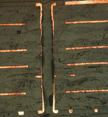
Tapered copper‑free holes share one typical feature: the copper coating on the hole wall gradually thins from the hole opening toward the hole centre and eventually disappears. Three commonly‑suspected causes are listed below:
- Poor throwing power of tin plating and defective tin coverage
- Abnormal PTH process failing to deposit copper inside holes
- Insufficient throwing power of copper electroplating
Countersink holes without copper plating are frequent defects in actual PCB production. The root cause lies in an inhibitory film formed on the conductive base copper (electroplated‑copper or heavy‑copper layer), which blocks subsequent copper electroplating. The formation mechanism and prevention methods are explained as follows.
After copper plating or heavy‑copper processing, PCBs proceed to circuit developing. Unpolymerized ink on the board surface dissolves inside the developer. The circulating pump sprays developer carrying ink macromolecules over the PCB surface and through holes. If the subsequent high‑pressure rinsing fails to thoroughly flush away residual ink macromolecules stuck on the board and hole walls, these polymer contaminants will adhere to inner hole walls and create a thin barrier film.
Rinsing weakens toward the hole centre, making barrier‑film formation far more likely, especially for tiny‑size holes. Multi‑stage rinsing after developing only dilutes residual pollutants rather than removing them completely.
Once polymer barrier films are confirmed as the main trigger for tapered thinning hole‑wall copper, the core solution is to strengthen hole‑wall cleaning and strip off the blocking layer. Effective treatment must target the fundamental cause.
Practical troubleshooting needs to take on‑site production constraints into consideration, such as shared developer for circuit and solder‑mask processes, mixed dry‑film and wet‑film workflows, and existing rinsing sequences.
Increased micro‑etching depth cannot eliminate the resist barrier layer inside holes. Excessive micro‑etching will even trigger copper‑free hole defects. The proper fixes include optimized developing and drying workflows, together with
High‑performance acidic degreaser for pre‑treatment before pattern transfer and metallization.
The EC‑51 acidic degreaser effectively resolves the gradual copper‑thinning issue from hole mouth to hole centre. Key operation specifications for EC‑51 are shown below:
- EC‑51 requires sufficient water rinsing. Residual wetting‑agent contaminants will generate excessive foam inside copper and nickel plating tanks.
- EC‑51 is originally formulated for wet‑film (black‑ink) workflows. It fixes non‑platable holes for copper and nickel plating. For fine‑pitch dry‑film circuits, reduce nozzle opening size and maintain EC‑51 concentration at 4%. Over‑high degreaser concentration will erode dry‑film edges and cause jagged copper traces. This chemical also works for copper‑free countersink‑hole issues under dry‑film processes.
- This defect occurs more often in cold winter months when low temperature weakens rinsing performance. Temperature adjustment delivers far better degreasing results than higher chemical concentration, which will only increase rinsing burdens. The recommended temperature range stays between 30‑35℃. Low temperatures weaken cleaning capacity, while over‑high temperature makes the degreaser penetrate and damage surface ink layers. For manual production lines, rock panels manually and run filtering systems to guarantee full chemical circulation inside through‑holes.