
What are the key processes of DIP post-soldering?
The DIP (Dual in-line Package) post-soldering process is an important link In the production of PCBA , which directly affects the reliability and performance of the product.
1. Plug-in preparation:
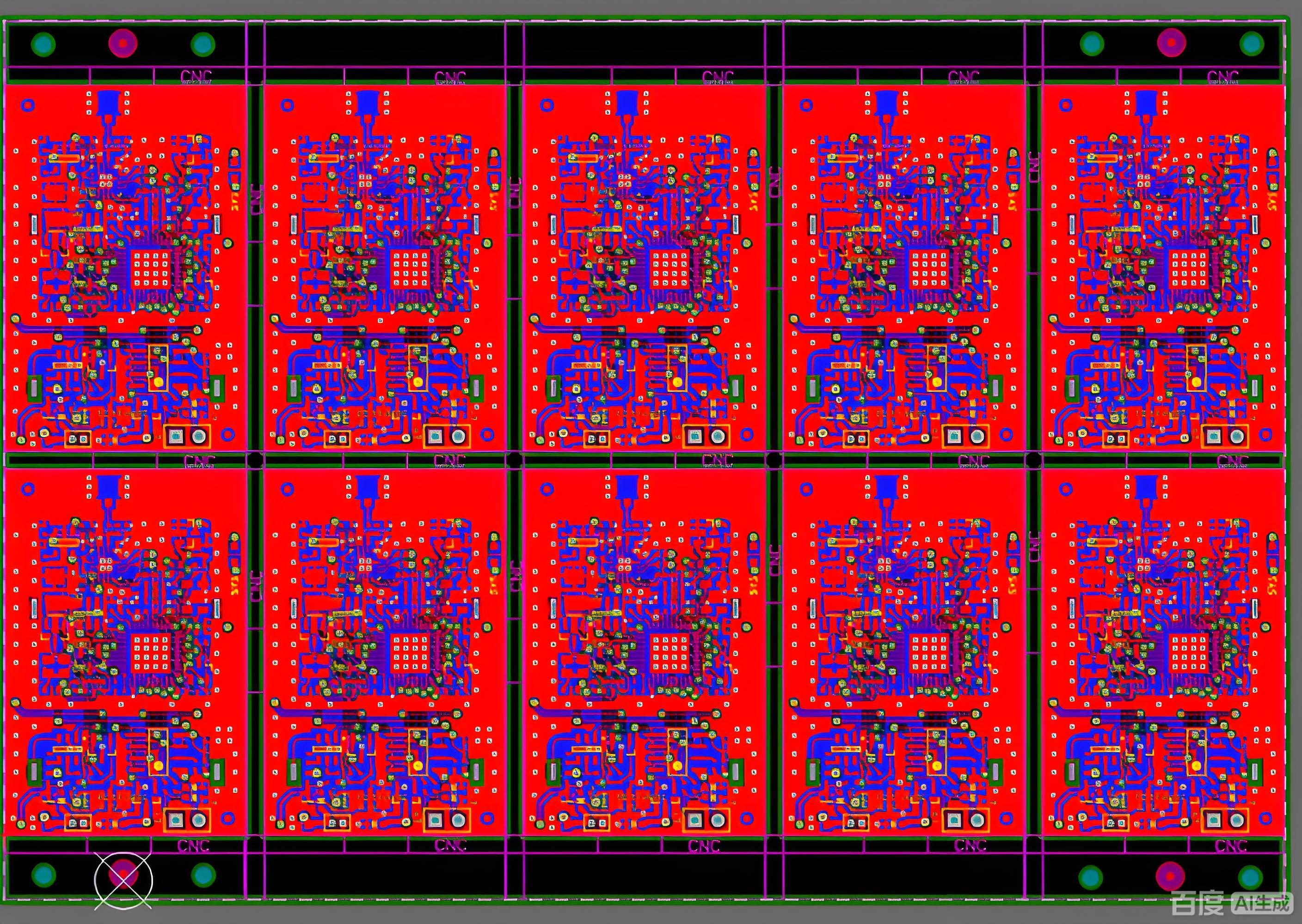
Manual plug-in: Experienced operators precisely insert through-hole components (such as electrolytic capacitors, connectors, etc.) into the corresponding holes on the PCB based on the BOM list.
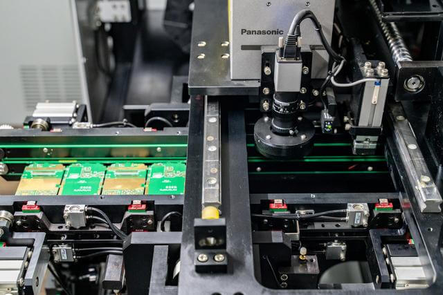
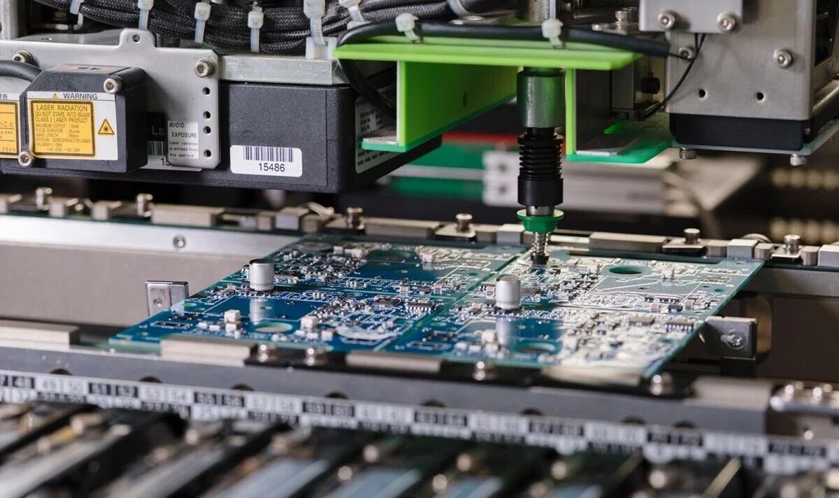
Automated assistance: Some high-precision plug-ins use semi-automatic equipment to ensure that the pins are aligned with the hole positions, avoiding skewing or floating height.
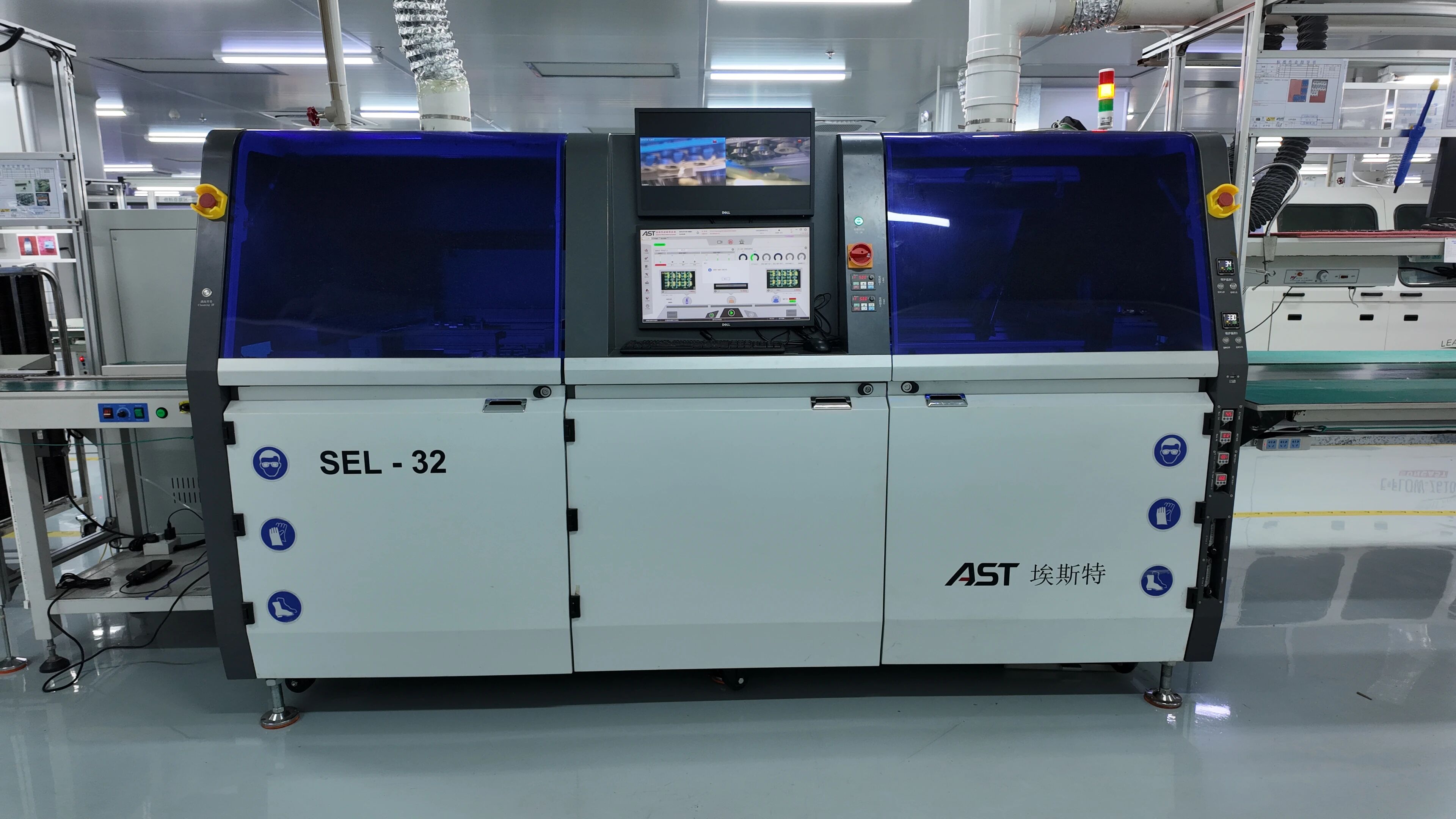
2.Wave soldering
Preheating stage :
The PCB passes through the preheating zone (100-150℃) to remove moisture from the board surface and reduce thermal shock during soldering.
Soldering stage: The molten solder forms a "wave peak" in the wave soldering machine, and the bottom of the PCB comes into contact with the solder, completing the metallurgical bonding of the pins and pads. Nitrogen protection: Asinda uses nitrogen wave soldering to reduce oxidation, enhance the brightness and reliability of solder joints.
3. Selective wave soldering:
For high-density boards or local soldering requirements, selective wave soldering equipment is used to precisely control the solder range and avoid thermal interference to adjacent components.
Difficulties and Solutions in DIP Post-welding Process
1. Causes of false soldering: Oxidation of solder pads, too small pin pitch or insufficient solder temperature.
Countermeasure: Xinjingfu detects the pad status through 3D SPI and strictly controls the furnace temperature curve (peak temperature 245±5℃).
2. Causes of bridging (short circuit) : Excessive soldering or unreasonable design of pin spacing.
Countermeasures: Optimize PCB design (such as adding solder mask Bridges), and adjust the dip Angle and flow rate of wave soldering.
3.damage to heat-sensitive components,
Countermeasures : Adopt local shielding or segmented welding techniques for components such as electrolytic capacitors to reduce thermal stress.
Advantages of Asinda DIP Post-welding
1. Strict workshop environment: 1000㎡ static protection workshop with real-time monitoring of temperature and humidity (22±2℃, humidity 40-60%) to prevent static damage and PCB moisture absorption.
2. Advanced equipment: guaranteed to be equipped with lead-free wave soldering, selective wave soldering and conformal coating equipment, supporting high-difficulty processes (such as thick plate welding and mixed plate processing).
3. 19 quality inspection procedures: from AOI inspection to X-RAY random inspection, ensure that the solder joints 100% comply with the IPC-A-610 Class 2/3 standard.

Typical application scenarios
1.industrial control equipment:such as relay welding of PLC modules, which requires vibration resistance and high reliability.
2.Medical electronics: The DIP welding of products such as defibrillators must pass the ISO13485 medical system certification.
3.Automotive electronics: High-temperature resistant solder joint process for on-board T-boxes, meeting the IATF16949 standard.