
The key to enhancing the high-voltage resistance of PCBA through welding processes lies in avoiding insulation failure or electric field concentration caused by welding defects.
The specific measures are as follows:
1. Control the shape of the solder joint to avoid the concentration of the electric field
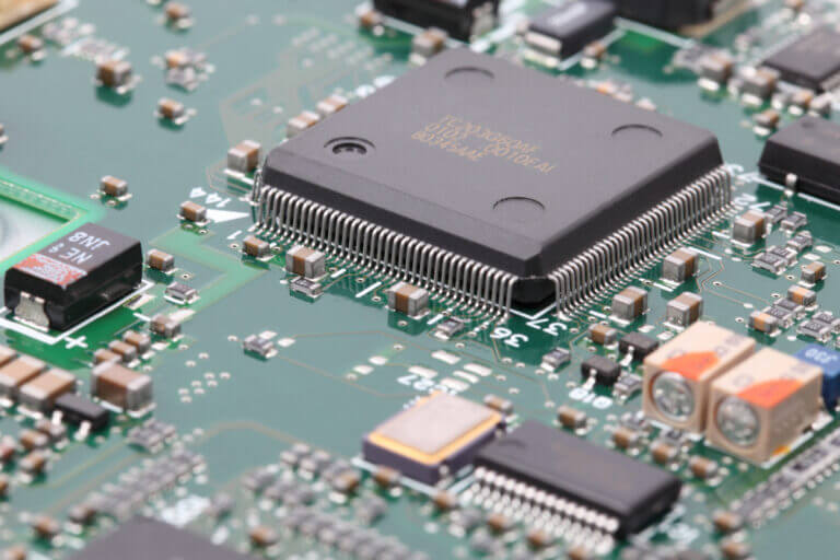
• Avoid sharp points and burrs: Solder joints in high-voltage areas (such as high-voltage capacitor pins and transformer pins) should be smooth and round, without any sharp protrusions. The tip can cause a sudden increase in the electric field intensity, which is prone to breakdown discharge. This can be achieved by optimizing the amount of solder and adjusting the temperature of the soldering iron (to prevent the solder from overheating and splashing).
• Ensure that the solder joints are full and free of voids: Voids can cause uneven distribution of the electric field near the solder joints. Under long-term high voltage, local overheating may lead to insulation aging. When soldering, it is necessary to ensure that the solder fully penetrates the pads and pins. This can be improved by pre-treating the oxide layer on the pins (such as tin plating) and controlling the soldering time (to avoid false soldering).
2.eliminate short circuits and insufficient creepage distance
• Prevent solder bridging: The pad spacing between high-voltage lines and low-voltage lines, as well as between different high-voltage nodes, must strictly comply with the design requirements. During soldering, avoid solder flowing to prevent bridging (a solder mask can be used for isolation or flux can be used to control solder fluidity).
• Clean up residual solder slag: After soldering, thoroughly remove excess solder and flux residues around the pads (especially rosin residues, which may carbonize and conduct electricity under high temperature and high pressure). Isopropyl alcohol can be used for cleaning to ensure the creepage path is clean.
3.Optimize welding materials and process parameters
• Select high-temperature resistant insulating solder: In high-pressure environments, high-melting-point solder (such as lead-tin alloy 63/37 or lead-free solder Sn-Ag-Cu) can be chosen to prevent the solder joints from melting due to long-term high temperatures. Choose fluxes with good insulation properties (such as no-clean fluxes) to reduce residual conductive substances.
• Control the soldering temperature and time: Excessively high temperatures may damage the insulation performance of the PCB substrate (such as a decrease in the Tg value of FR-4 substrate). Parameters should be set based on the temperature resistance of the PCB and components (such as a general component soldering temperature of 250-300℃ and a time of 3-5 seconds) to prevent substrate carbonization or delamination.
4. Strengthen welding protection in high-voltage areas
• Isolated soldering operation: Soldering in the high-voltage area and the low-voltage area should be carried out separately to avoid cross-contamination (such as solder residue from the low-voltage area splashing into the high-voltage area).
• Insulation reinforcement is adopted: For high-voltage solder joints, additional insulating glue (such as silicone rubber) can be applied or insulating sleeves can be put on to further enhance the insulation isolation between the solder joints and the surrounding environment, especially suitable for damp and dusty working conditions.
 Through the above measures, the weak points of insulation can be reduced in the welding process.
Combined with PCB design and material selection, the high-voltage stability of the PCBA can be significantly enhanced.