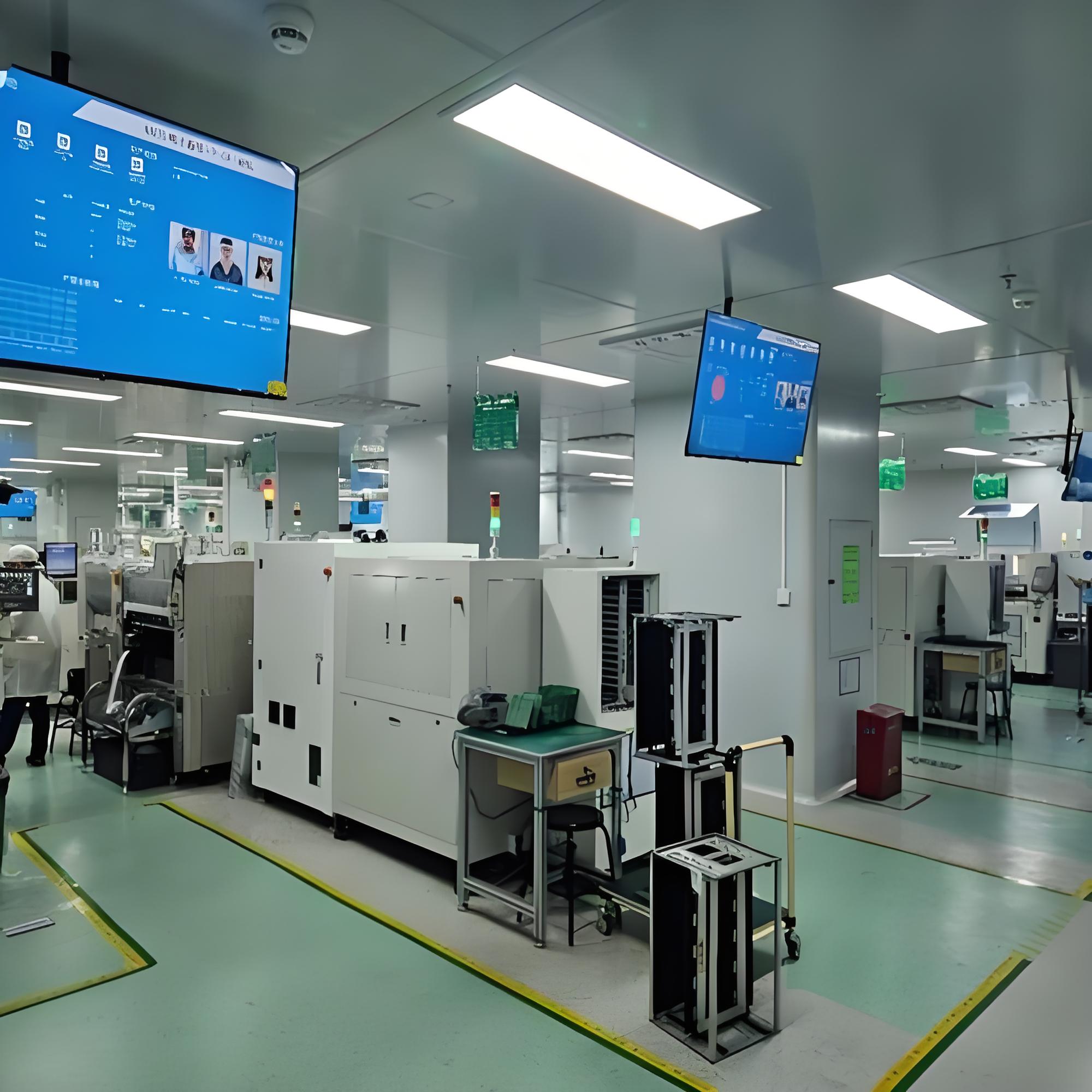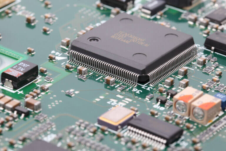

In PCB manufacturing and SMT (surface mount technology) processing, the assembly is a crucial link. It not only affects the production efficiency, cost effectiveness, but also directly related to the quality and stability of the final product.
First, why should PCB be panelized?
1. Improve production efficiency
• Reduce the number of refueling: Through the assembly, multiple small PCB are combined into a whole, reducing the number of frequent refueling in the machine during the process, thereby improving the overall production efficiency.
• Simplified machining process: The panelized PCB can be more easily processed and assembled, such as the alignment of multiple small board connectors, which is convenient for subsequent testing and repair work.
2. Reduce costs
• Improve material utilization: For shaped or low area utilization of PCB , panels can more effectively use the board area, reduce waste, improve cost utilization.
• Reduce mounting costs: The patchwork design can reduce the mounting cost of a single PCB and improve the efficiency of the mounting head of the SMT machine.
3. Improve mounting accuracy
• Reduce cumulative errors: The panel design reduces cumulative errors in handling and positioning, thereby improving the accuracy of component mounting.
• Optimized logistics storage: Large size panels simplify handling and storage, reducing the risk of damage due to improper operation.
4. Adapt to automated production
• Improve the level of automation: The panel design can better adapt to the automated production line, improve the automation level of the production process, reduce the manual operation and the risk of error and damage.
5. Easy to test and inspect
• Quick problem detection: Checking multiple PCBS at the same time can quickly identify potential problems and improve production efficiency and quality control.
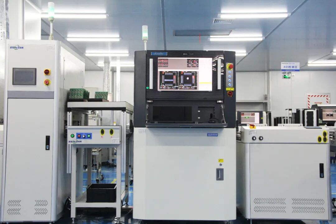
Second, SMT machine requirements for PCB size SMT machine has strict requirements for PCB board size to ensure the accuracy and production efficiency of the patch. Here are some of the main size requirements:
1. Panel size limit
In general, the width of the PCB assembly should be less than or equal to 260mm (SIEMENS line) or 300mm (FUJI line). If automatic dispensing operation is required, the width x length of the board should be less than or equal to 125mm x 180mm.
2. Panel shape design
When designing the plate, the shape should be designed as square or a rectangle close to the square as possible to improve the utilization rate and processing efficiency of the plate.
3. Panel frame design
The outer frame (process edge) of the circuit board after the assembly shall adopt a closed-loop design to ensure that there will be no deformation after the PCB assembly is fixed on the fixture.
4. Spacing and positioning of small boards
The center distance between the small plates should be controlled between 75mm and 145mm to ensure the convenience of processing and assembly.
Each small board shall be provided with three or more positioning holes, the aperture is between 3mm and 6mm, the edge positioning holes within 1mm cannot be wired or SMT.
5. Mark Point design
The Mark point is a key positioning benchmark in SMT chip processing, and its shape, size, position and surrounding environment have strict requirements. Mark points are typically standard circles, squares, or triangles with sizes between 0.8mm and 1.5mm to ensure fast and accurate capture by visual recognition systems.
6. Other requirements
Four positioning holes should be opened at the four corners of the outer frame of the plate, and the aperture is generally 4mm±0.01mm, and the strength of the hole should be appropriate to ensure that there will be no bad phenomena such as fracture during the processing of the SMT patch.
Within the range that SMT equipment can handle, the overall size of the PCB board is usually between 50mm×50mm and 350mm×250mm.
The bending and deformation of PCB board will seriously affect the quality of SMT patch processing, so it is necessary to strictly control its bending and distortion.