Blind and buried via PCB refers to the use of blind and buried via technology to connect circuits on different layers in PCB, thereby achieving higher density wiring and more compact design.
What are blind and buried vias?
Blind Via: A blind via is a hole that extends from the surface layer of a PCB to an inner layer but does not penetrate the entire board. This hole is only visible on one side of the board and is usually used to connect circuits on the surface layer and the inner layer.
Buried Via: Buried Via refers to a hole that is completely buried inside the PCB. It is only used to connect the circuits of the internal layers and cannot be seen from the outside. This type of hole can further increase the number of layers and wiring density of the circuit board.
Advantages of Blind and Buried Via PCB
1. Multilayer structure: The multilayer structure of blind and buried via PCB can have 4, 6 or even more layers. Through the design of blind and buried vias, more circuit connections can be achieved in a limited space.
2. High-density wiring: Blind and buried via technology can achieve higher line density in a smaller area, allowing the circuit board to accommodate more components and more complex circuit designs.
3. Reduce size: Due to the use of blind and buried vias, the space waste caused by traditional through-holes can be reduced, thereby reducing the size of the circuit board and adapting to the miniaturization requirements of modern electronic products.
4. Improve electrical performance: The design of blind and buried vias can optimize the signal transmission path, reduce signal delay and crosstalk, and improve signal integrity and electrical performance, which is particularly suitable for high-speed signal transmission application scenarios.
5. Improve reliability: By reducing the number of holes and optimizing wiring, blind and buried via PCBs can reduce stress concentration points during the manufacturing process and improve the mechanical strength and reliability of the circuit board.
Technical Difficulties of Blind and Buried Via PCB
1. Drilling accuracy
Difficulty: Drilling of blind and buried vias requires extremely high precision to avoid hole offset and inconsistent size. Especially for blind vias, the drilling depth needs to be precisely controlled, and the error must be within the micron level.
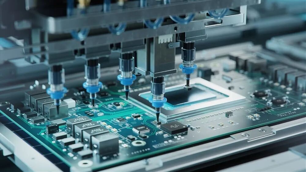
Solution: In order to ensure the accuracy of drilling, laser drilling technology is used in the manufacturing process. Laser drilling has the following advantages:
High precision: Laser drilling can achieve precise hole diameter and depth control in a small area with minimal error.
Non-contact processing: Laser drilling does not require contact with the material, reducing mechanical stress and hole wall damage, and avoiding the offset and deformation that may be caused by traditional mechanical drilling.
Automated control: Laser drilling equipment is equipped with an advanced automated control system that can accurately set the position and depth of each hole to ensure consistency.
2.Electroplating and via filling
Difficulty: The electroplating process of blind and buried vias needs to ensure that the hole wall is evenly covered with copper to ensure the reliability of electrical connection. Avoid bubbles and incomplete filling during the hole filling process, as these defects will affect the conductivity and mechanical strength.
Solution:
Chemical plating and electrolytic plating: Chemical plating can deposit a uniform copper layer on the hole wall to ensure the conductivity inside the blind and buried holes. Electrolytic plating is then performed to further enhance the thickness and strength of the copper layer.
Vacuum hole filling technology: In order to avoid bubbles and incomplete filling during the hole filling process, vacuum hole filling technology is used. Hole filling in a vacuum environment can effectively remove bubbles in the hole and ensure uniform distribution of the filling material.
High-quality hole filling materials: Using highly conductive and highly viscous hole filling materials can further improve the hole filling effect and ensure electrical performance and mechanical strength.
3.Lamination and pressing
Difficulty: Multi-layer blind buried hole PCBs are prone to problems such as misalignment, separation and bubbles during lamination and pressing. Any slight misalignment or separation will affect the integrity and performance of the circuit.
Solution:
High-precision alignment equipment: Using high-precision alignment equipment can ensure the precise alignment of each layer. Alignment equipment is usually equipped with an automatic alignment system, which uses optical or laser positioning technology to achieve precise matching between layers.
High-pressure pressing technology: During the pressing process, high-pressure equipment and precise temperature control are used to ensure that the layers are tightly combined to avoid separation and bubbles between layers. High-pressure pressing can effectively eliminate air between layers and improve interlayer bonding.
High-quality laminating materials: Selecting high-quality laminating materials, such as high-performance epoxy resins, can improve the bonding strength and heat resistance between layers, and further ensure the effect of lamination and pressing.
Application scenarios of blind and buried via PCB
Consumer electronics:
Smartphones, tablets, wearable devices: high-density wiring and miniaturized design to achieve high functional integration and high performance.
Communication equipment:
5G base stations, optical communication equipment: excellent signal integrity and high precision, supporting high-speed data processing and signal transmission.
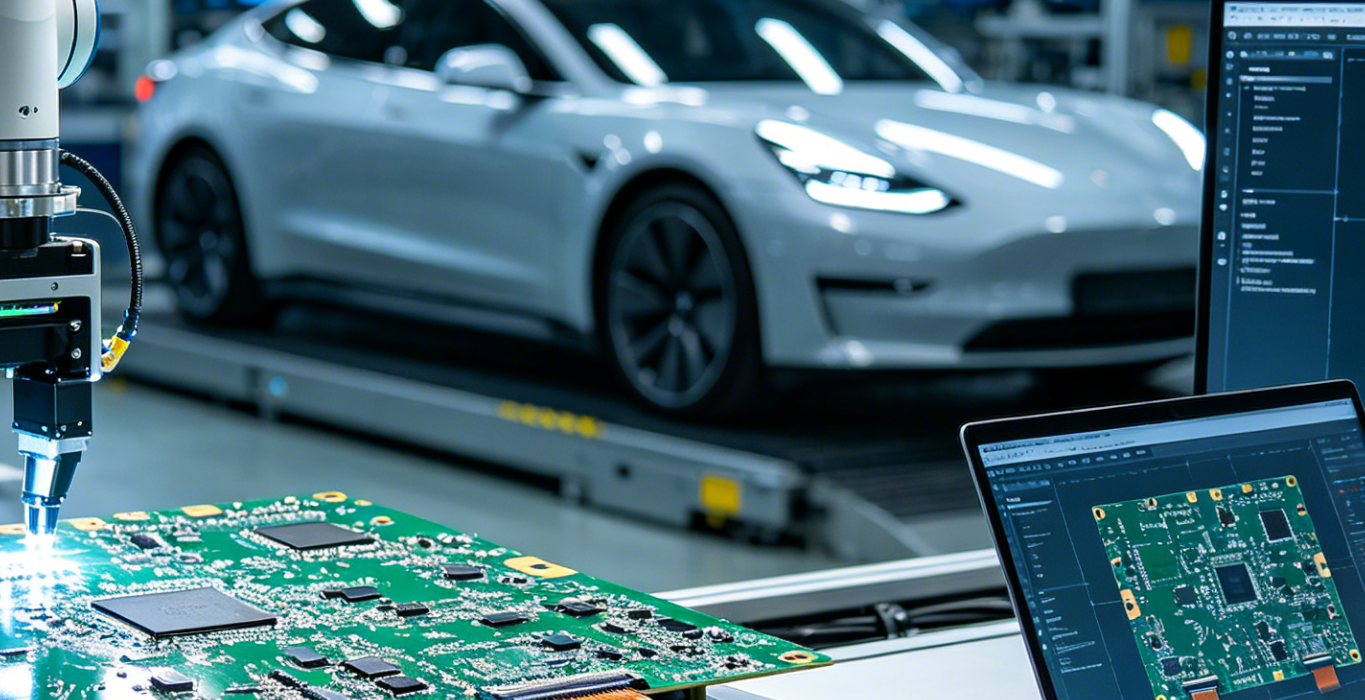
Automotive electronics:
Automotive control systems, in-vehicle entertainment systems: high mechanical strength and multi-functional integration to ensure system stability and improve entertainment quality.
Medical equipment:
Portable medical equipment, medical imaging equipment: miniaturized design and high-precision image processing to meet high performance requirements.
High-performance computing:
Servers and data centers, artificial intelligence computing equipment: multi-layer structure and high-performance support to meet high-speed data processing and complex computing requirements.
Asinda has 17 years of experience in PCB manufacturing, specializing in the production of various high-layer precision circuit boards, blind and buried via boards, high-frequency boards, hybrid laminates, metal substrates, rigid-flex boards, etc. If you need, you can contact us at any time.
