Our Free DFM Check helps you identify potential manufacturability issues in your PCB design before production. Avoid costly errors, improve design efficiency, and speed up your project timeline with our expert analysis.
Upload file
Submit Your Design for a Free DFM Check
Why a Free DFM Check is Essential for Your PCB Design?
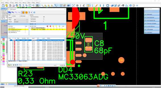
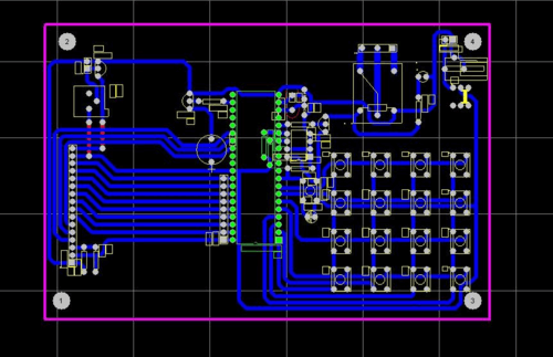
A Design for Manufacturability (DFM) check is a crucial step in the PCB design process, particularly for complex designs. This service helps engineers identify and rectify potential issues during the design phase that could negatively impact manufacturing. By implementing a DFM check, you can ensure a smoother production process and avoid costly mistakes later on.
Identifying Design Errors
One of the primary benefits of a DFM check is its ability to identify design errors early in the development cycle. Without this proactive approach, engineers might overlook critical issues that lead to unnecessary rework during production. Common design mistakes include incompatible component layouts and improperly sized traces, which can significantly impact the overall functionality of the PCB. By catching these errors in advance, you save time and resources, allowing for a more efficient workflow.
Improving PCB Manufacturability
A DFM check enhances the manufacturability of your PCB, ultimately reducing production delays. By optimizing your design for manufacturing, you ensure that the PCB can be produced using standard processes and techniques. This means fewer complications during assembly and a faster turnaround time from design to production. When designs are straightforward and manufacturable, manufacturers can maintain consistent quality and keep lead times short.
Lowering Manufacturing Costs
Another significant advantage of a DFM check is the potential for cost reduction. By identifying issues that could complicate the manufacturing process, you can make adjustments that optimize material usage and component layout. This not only reduces waste but also minimizes labor costs associated with fixing design flaws during production. A well-optimized PCB design translates directly into lower manufacturing expenses and improved profit margins.
Common Issues Without a DFM Check
Without a DFM check, several common problems can arise, hindering the efficiency of your PCB design:
Incompatible Component Layouts: Designs may include components that are not compatible with each other, leading to assembly failures and increased rework.
Trace Width Issues: Traces that are too wide or too narrow can lead to power loss, signal integrity problems, or even physical damage during manufacturing.
Poor Pad Design: Inadequately designed pads can result in weak solder joints or improper component placement, risking overall functionality and reliability.
We are committed to making our products zero-defect and can return or exchange them for you without any reason.
Sign up for our newsletter to receive updates, news, insights, and promotions.
Terms & Conditions Privacy Policy
Services
Support
Company
Get In Touch
Head office : Chang'an Building, No. 56, Second Industrial Zone, Houting Community, Shajing Street, Bao'an District, Shenzhen Factory address:6-8/F, Building 6 Plant, No. 319 Longxi Road, Jianghai District, Jiangmen City, Guangdong Province